
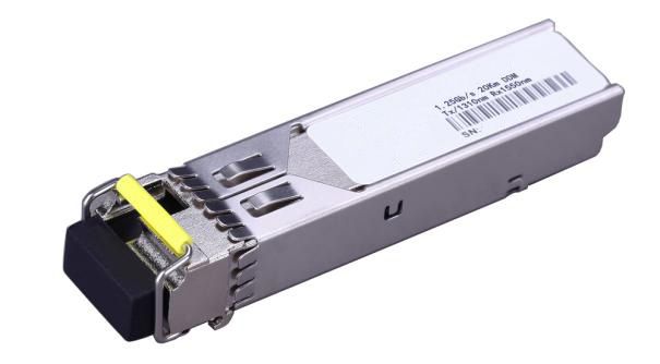
讯艾拓XAT-GW20-15光模块 Transceivers are a high performance, cost effective module which have a single LC optics interface. They are compatible with the Small Form Factor Pluggable Multi-Sourcing Agreement (MSA) and Digital diagnostics functions are available via the 2-wire serial bus specified in SFF-8472. The receiver section uses a PIN receiver and the transmitter uses a 1310 nm FP laser, up to 14dB link budge ensure this module 1000Base-LX Ethernet 20km application.
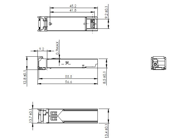
二、产品特点:² Up to 1.25Gb/s Data Links
² Hot-Pluggable
² Single LC connector
² Up to 20 km on 9/125μm SMF
² 1550nm FP laser transmitter
²1310nm PIN photo-detector
² Single +3.3V Power Supply
² Monitoring Interface Compliant with SFF-8472
² Maximum Power <1W
² Industrial /Extended/ Commercial operating temperature range: -40°C to 85°C/-5°C to 85°C/-0°C to 70°C Version available
² RoHS compliant and Lead Free
Applications:
² 1000Base-LX Ethernet
² Metro/Access Networks
² 1×Fibre Channel
Other Optical Links
|
Parameter |
Symbol |
Min. |
Typical |
Max. |
Unit |
|
Storage Temperature |
TS |
-40 |
|
+85 |
°C |
|
Supply Voltage |
VCC |
-0.5 |
|
4 |
V |
|
Relative Humidity |
RH |
0 |
|
85 |
% |
|
Parameter |
Symbol |
Min. |
Typical |
Max. |
Unit |
|
|
Case operating Temperature |
Industrial |
TC |
-40 |
|
85 |
°C |
|
Extended |
-5 |
|
85 |
°C |
||
|
Commercial |
0 |
|
+70 |
°C |
||
|
Supply Voltage |
VCC |
3.135 |
|
3.465 |
V |
|
|
Supply Current |
Icc |
|
|
300 |
mA |
|
|
Inrush Current |
Isurge |
|
|
Icc+30 |
mA |
|
|
Maximum Power |
Pmax |
|
|
1 |
W |
|
|
Parameter |
Symbol |
Min. |
Typical |
Max. |
Unit |
Note |
|
Transmitter Section: |
|
|||||
|
Input differential impedance |
Rin |
90 |
100 |
110 |
W |
1 |
|
Single ended data input swing |
Vin PP |
250 |
|
1200 |
mVp-p |
|
|
Transmit Disable Voltage |
VD |
Vcc – 1.3 |
|
Vcc |
V |
2 |
|
Transmit Enable Voltage |
VEN |
Vee |
|
Vee+ 0.8 |
V |
|
|
Transmit Disable Assert Time |
Tdessert |
|
|
10 |
us |
|
|
Receiver Section: |
|
|||||
|
Single ended data output swing |
Vout,pp |
250 |
|
800 |
mv |
3 |
|
LOS Fault |
Vlosfault |
Vcc – 0.5 |
|
VCC_host |
V |
5 |
|
LOS Normal |
Vlos norm |
Vee |
|
Vee+0.5 |
V |
5 |
|
Power Supply Rejection |
PSR |
100 |
|
|
mVpp |
6 |
Note:
1. AC coupled.
2. Or open circuit.
3. Into 100 ohm differential termination.
4. 20 – 80 %
5. LOS is LVTTL. Logic 0 indicates normal operation; logic 1 indicates no signal detected.
6. All transceiver specifications are compliant with a power supply sinusoidal modulation of 20 Hz to 1.5MHz up to specified value applied through the power supply filtering network shown on page 23 of the Small Form-factor Pluggable (SFP) Transceiver Multi-Source Agreement (MSA), September 14, 2000.
Optical Parameters(TOP = -40 to 85°C, VCC = 3.135 to 3.465 Volts):
|
Parameter |
Symbol |
Min. |
Typical |
Max. |
Unit |
Note |
|
Transmitter Section: |
||||||
|
Center Wavelength |
λc |
1270 |
1310 |
1600 |
nm |
|
|
Spectral Width(RMS) |
σRMS |
|
|
4 |
nm |
|
|
Optical Output Power |
Pout |
-9 |
|
-3 |
dBm |
1 |
|
Extinction Ratio |
ER |
9 |
|
|
dB |
|
|
Optical Rise/Fall Time |
tr / tf |
|
|
260 |
ps |
2 |
|
Relative Intensity Noise |
RIN |
|
|
-120 |
dB/Hz |
|
|
Total Jitter Contribution |
TX Δ TJ |
|
|
0.284 |
UI |
3 |
|
Eye Mask for Optical Output |
Compliant with IEEE802.3 z (class 1 laser safety) |
|
||||
|
Receiver Section: |
|
|||||
|
Optical Input Wavelength |
λc |
1530 |
1550 |
1570 |
nm |
|
|
Receiver Overload |
Pol |
-3 |
|
|
dBm |
4 |
|
RX Sensitivity |
Sen |
|
|
-24 |
dBm |
4 |
|
RX_LOS Assert |
LOS A |
-40 |
|
|
dBm |
|
|
RX_LOS De-assert |
LOS D |
|
|
-25 |
dBm |
|
|
RX_LOS Hysteresis |
LOS H |
0.5 |
|
|
dB |
|
|
General Specifications: |
||||||
|
Data Rate |
BR |
|
1.25 |
|
Gb/s |
|
|
Bit Error Rate |
BER |
|
|
10-12 |
|
|
|
Max. Supported Link Length on 9/125μm SMF@1.25Gb/s |
LMAX |
|
20 |
|
km |
|
|
Total System Budget |
LB |
14 |
|
|
dB |
|
Note
1.The optical power is launched into SMF.
2.20-80%.
3.Contributed total jitter is calculated from DJ and RJ measurements using TJ = RJ + DJ. Contributed RJ is calculated for 1x10-12 BER bymultiplying the RMS jitter (measured on a single rise or fall edge) from the oscilloscope by 14. Per FC-PI (Table 9 - SM jitter output, note 1), the actual contributed RJ is allowed to increase above its limit if the actual contributed DJ decreases below its limits, as long as the component output DJ and TJ remain within their specifi ed FC-PI maximum limits with the worst case specified component jitter input.
4.Measured with PRBS 27-1 at 10-12 BER
Pin Assignment:
Diagram of Host Board Connector Block Pin Numbers and Name
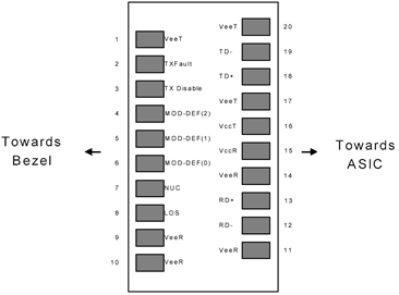
Diagram of Host Board Connector Block Pin Numbers and Names
Pin Function Definitions:
|
Pin No |
Name |
Function |
Plug Seq |
Notes |
|
1 |
VeeT |
Transmitter Ground |
1 |
1 |
|
2 |
TX Fault |
Transmitter Fault Indication |
3 |
|
|
3 |
TX Disable |
Transmitter Disable |
3 |
2 |
|
4 |
MOD-DEF2 |
Module Definition |
2 |
3 |
|
5 |
MOD-DEF1 |
Module Definition 1 |
3 |
3 |
|
6 |
MOD-DEF0 |
Module Definition 0 |
3 |
3 |
|
7 |
Rate Select |
Not Connected |
3 |
4 |
|
8 |
LOS |
Loss of Signal |
3 |
5 |
|
9 |
VeeR |
Receiver Ground |
1 |
1 |
|
10 |
VeeR |
Receiver Ground |
1 |
1 |
|
11 |
VeeR |
Receiver Ground |
|
1 |
|
12 |
RD- |
Inv. Received Data Out |
3 |
6 |
|
13 |
RD+ |
Received Data Out |
3 |
6 |
|
14 |
VeeR |
Receiver Ground |
3 |
1 |
|
15 |
VccR |
Receiver Power |
2 |
1 |
|
16 |
VccT |
Transmitter Power |
2 |
|
|
17 |
VeeT |
Transmitter Ground |
1 |
|
|
18 |
TD+ |
Transmit Data In |
3 |
6 |
|
19 |
TD- |
Inv. Transmit In |
3 |
6 |
|
20 |
VeeT |
Transmitter Ground |
1 |
|
Notes:
1. Circuit ground is internally isolated from chassis ground.
2. Laser output disabled on TDIS >2.0V or open, enabled on TDIS <0.8V.
3. Should be pulled up with 4.7k - 10 kohms on host board to a voltage between 2.0V and 3.6V. MOD_DEF(0) pulls line low to indicate module is plugged in.
4. Rate select is not used
5. LOS is open collector output. Should be pulled up with 4.7k – 10 kohms on host board to a voltage between 2.0V and 3.6V. Logic 0 indicates normal operation; logic 1 indicates loss of signal.
6.AC Coupled
SFP Module EEPROM Information and Management: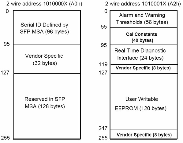
|
Data Address |
Length (Byte) |
Name of Length |
Description and Contents |
|
Base ID Fields |
|||
|
0 |
1 |
Identifier |
Type of Serial transceiver (03h=SFP) |
|
1 |
1 |
Reserved |
Extended identifier of type serial transceiver (04h) |
|
2 |
1 |
Connector |
Code of optical connector type (07=LC) |
|
3-10 |
8 |
Transceiver |
|
|
11 |
1 |
Encoding |
NRZ(03h) |
|
12 |
1 |
BR, Nominal |
Nominal baud rate, unit of 100Mbps |
|
13-14 |
2 |
Reserved |
(0000h) |
|
15 |
1 |
Length(9um) |
Link length supported for 9/125um fiber, units of 100m |
|
16 |
1 |
Length(50um) |
Link length supported for 50/125um fiber, units of 10m |
|
17 |
1 |
Length(62.5um) |
Link length supported for 62.5/125um fiber, units of 10m |
|
18 |
1 |
Length(Copper) |
Link length supported for copper, units of meters |
|
19 |
1 |
Reserved |
|
|
20-35 |
16 |
Vendor Name |
SFP vendor name: XAT |
|
36 |
1 |
Reserved |
|
|
37-39 |
3 |
Vendor OUI |
SFP transceiver vendor OUI ID |
|
40-55 |
16 |
Vendor PN |
Part Number: “XAT-GW20-15” (ASCII) |
|
56-59 |
4 |
Vendor rev |
Revision level for part number |
|
60-62 |
3 |
Reserved |
|
|
63 |
1 |
CCID |
Least significant byte of sum of data in address 0-62 |
|
Extended ID Fields |
|||
|
64-65 |
2 |
Option |
Indicates which optical SFP signals are implemented (001Ah = LOS, TX_FAULT, TX_DISABLE all supported) |
|
66 |
1 |
BR, max |
Upper bit rate margin, units of % |
|
67 |
1 |
BR, min |
Lower bit rate margin, units of % |
|
68-83 |
16 |
Vendor SN |
Serial number (ASCII) |
|
84-91 |
8 |
Date code |
XAT’s Manufacturing date code |
|
92-94 |
3 |
Reserved |
|
|
95 |
1 |
CCEX |
Check code for the extended ID Fields (addresses 64 to 94) |
|
Vendor Specific ID Fields |
|||
|
96-127 |
32 |
Readable |
XAT specific date, read only |
|
128-255 |
128 |
Reserved |
Reserved for SFF-8079 |
|
Data Address |
Parameter |
Accuracy |
Unit |
|
96-97 |
Transceiver Internal Temperature |
±3.0 |
°C |
|
100-101 |
Laser Bias Current |
±10 |
% |
|
100-101 |
Tx Output Power |
±3.0 |
dBm |
|
100-101 |
Rx Input Power |
±3.0 |
dBm |
|
100-101 |
VCC3 Internal Supply Voltage |
±3.0 |
% |
The XAT-GW20-15 complies with international Electromagnetic Compatibility (EMC) and international safety requirements and standards (see details in Table following).
XAT-GM02-15
1.25Gb/s 20Km LC BiDi SFP Transceiver
Hot Pluggable, Single LC, +3.3V, 1550nm Tx/1310nm Rx, DFB-LD, Single-mode, DDM